AO6601
Overview
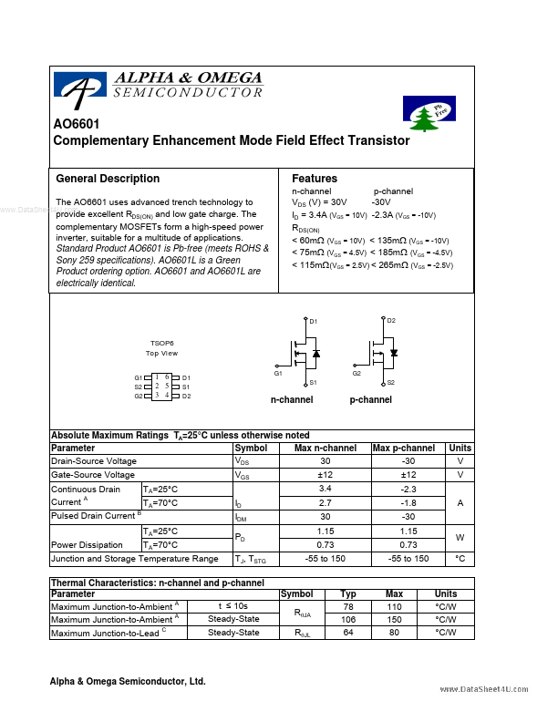
The AO6601 uses advanced trench technology to provide excellent RDS(ON) and low gate charge. The complementary MOSFETs form a high-speed power inverter, suitable for a multitude of applications.
| Part | AO6601 |
|---|---|
| Description | MOSFET |
| Category | MOSFET |
| Manufacturer | Alpha & Omega Semiconductors |
| Size | 240.23 KB |
The AO6601 uses advanced trench technology to provide excellent RDS(ON) and low gate charge. The complementary MOSFETs form a high-speed power inverter, suitable for a multitude of applications.
| Part Number | Manufacturer | Description |
|---|---|---|
| AO6601 | VBsemi | N- and P-Channel 20V MOSFET |
| AO6604 | VBsemi | Dual-Channel MOSFET |